The Ubiquitous Microwave Diode. Chapter 2: PIN Diodes
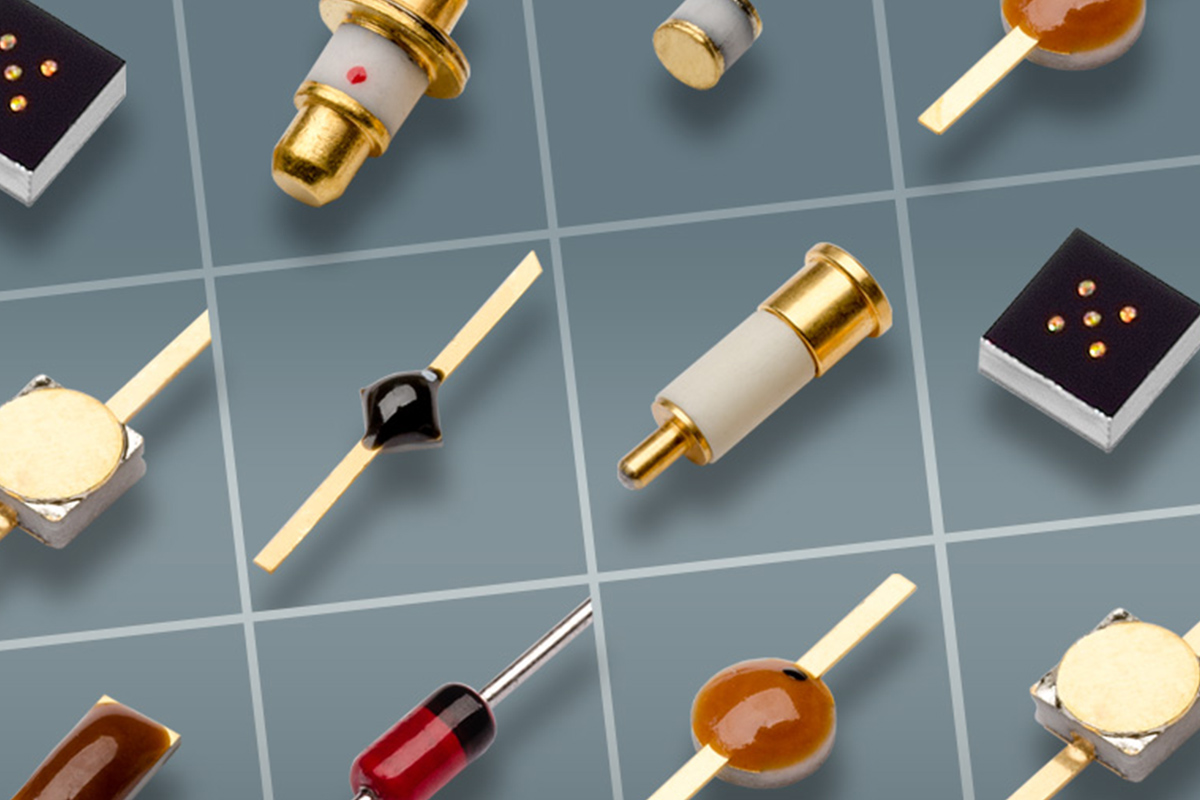
The PIN diode is one of the most versatile types for RF and Microwave designers, which is why it’s used in a broad array of applications from limiters to phase shifters, modulators, attenuators, and switches. In this article we’ll show you how they work and why they’re so well suited for microwave applications.
The "PIN" acronym comes from the diode’s P-type, intrinsic, and N-type semiconductor materials (Figure 1).
It was first realized in silicon in the early 1950s at low frequencies as a rectifier and microwave applications began to take off in the coming decade. Current PIN diodes are made of gallium arsenide as well. The intrinsic layer is what allows a PIN diode to have desirable characteristics such as a high reverse breakdown voltage, low capacitance, and carrier storage (when forward biased), that make it appealing for microwave applications. When compared to basic PN junction diodes, PIN diodes are more linear, reducing spurious signals, and when reverse biased they have greater isolation when acting as switching or attenuation elements.
Figure 1
A PIN diode will act as a rectifier at lower frequencies but at HF frequencies and above, they become purely resistive, the resistance value depending on depends on the applied DC bias current. The frequency at which this occurs depends on the thickness of the diode’s intrinsic region, and the greater the thickness the lower the frequency at which it takes place.
Modulators
When a PIN diode is used as a switching or attenuating element, only one signal or a band of signals are present. However, when a PIN diode is used as a modulator element two signals are simultaneously present – a carrier and a much lower-frequency signal that represents a slowly-varying bias current that modulates the impedance in the diode’s intrinsic region that the diode present to the carrier, which causes carrier wave’s amplitude to change. In addition to amplitude, the carrier wave’s frequency and phase can also be modulated.
Limiters
PIN diodes can be used to create the limiters used to protect sensitive components such as low noise amplifiers (LNAs) in a receiver from high signal levels. The PIN diode is placed as a shunt across the transmission path to the receiver front end. When input signals reach a specific amplitude, the diode’s junction resistance drops two a very low value, shorting out the transmission line in the limiter circuit. It essentially acts as a reflective switch, sending the signal back to the source, protecting any circuit a device forward from the limiter. Once the signal is no longer present, the diode returns to its former state.
Attenuators
PIN diodes can be used to make quadrature hybrid, quarter-wave, and other types of attenuators by using them in place of variable resistances. They use the forward biased resistance of the device over nearly its complete forward bias range. PIN diode attenuator circuits are used in automatic gain control (AGC) circuits and power leveling applications. They can be formed as a simple a series or shunt diode mounted across the transmission line but more often are networks that maintain an impedance match to both the input and output as attenuation is varied (Figure 2).
Figure 2
Phase shifters
The high-speed switching between on and off impedance states make the PIN diode well suited for useful for many types of high-speed phase shifters, where they are used as series- or shunt-connected switches. The switched elements are either lengths of transmission line or reactive elements. A PIN diode can be considered a lumped variable-impedance component and signals passing through them shift in phase. A lumped element representation permits the design of compact phase shifter circuits at the RF frequency bands but at higher frequencies insertion loss and power-handling ability decrease.
Switches
The operation of PIN diodes used as switching elements is based on the difference between the diode’s reverse and forward bias characteristics. The diode exhibits very low impedance under forward bias and a very large impedance when reverse biased, the difference in characteristics difference between them provides the switching function. Power handling ability is a key metric in RF power switching, as is isolation (how effectively the diode is turned off), and insertion loss. Isolation can be increased when two or more diodes are connected in series, which also allows the devices to share the same bias current, reducing power consumption.
Among the many types of diodes, the PIN diode continue to play a major role in the subsystems described above as well as others, even while digital circuits performing functions such as phase shifters are increasingly used. The next blog in this series describes step-recovery diodes, which are a lot different than PIN and other diodes.
Check out more of our blogs, including "The Ubiquitous Microwave Diode. Chapter 1: Schottky Diodes" and keep a look out for Chapter 3.
Contact our technical support team with any questions.
Captions
1. The three layers of a PIN diode
2. A matched coupler using two diodes.