The Ubiquitous Microwave Diode. Chapter 1: Schottky Diodes
The Schottky-barrier diode has become a staple in the microwave designer’s toolkit because its performance is closer to an “ideal” diode than many other types. In this blog, we’ll show you its advantages and disadvantages.
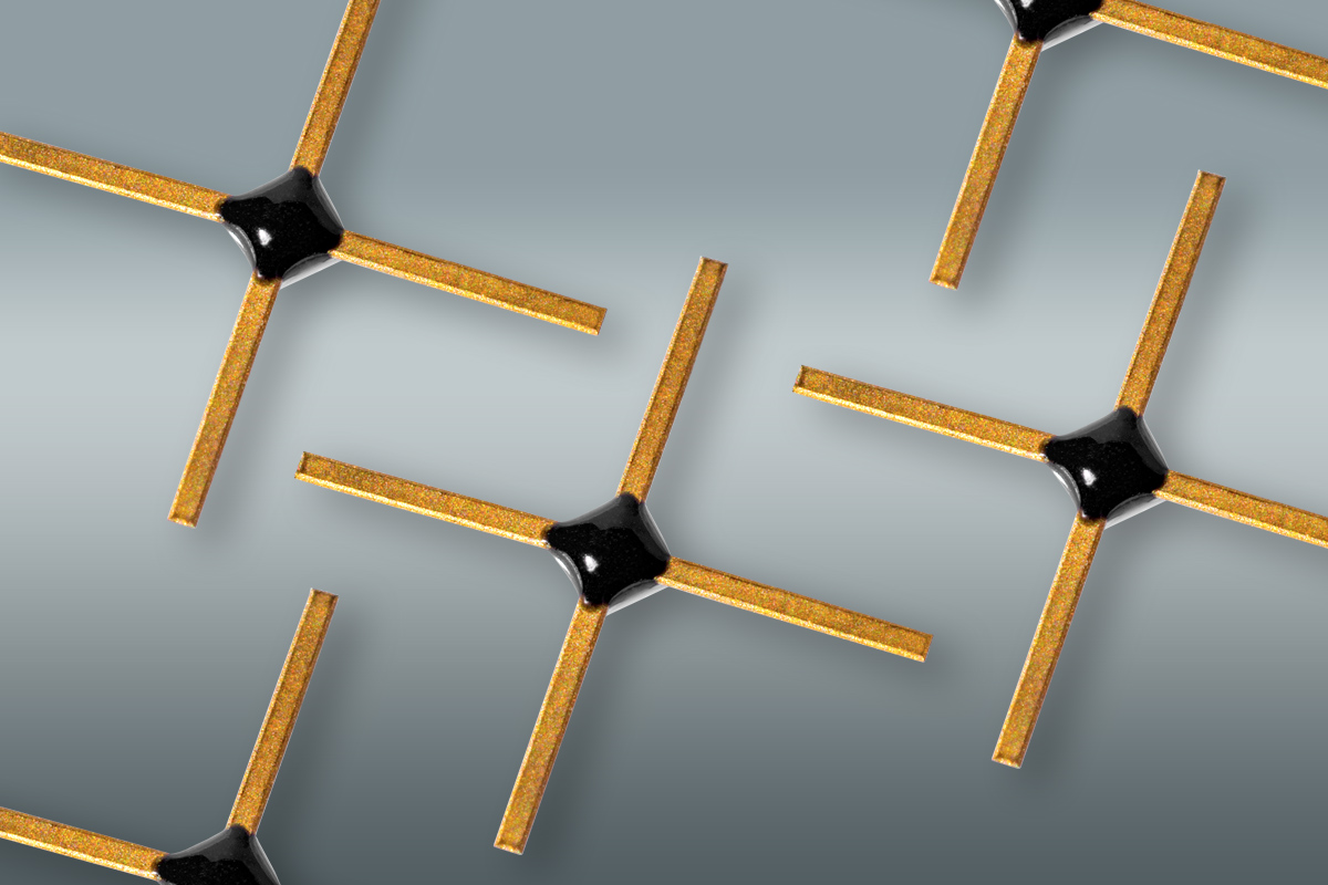
For this versatile device, we have Walter Hans Schottky to thank. Schottky (1886-1976) was a prolific German physicist who patented the superheterodyne principle for receiving wireless signals, and invented the ribbon microphone and loudspeaker, the screen-grid, tetrode and pentode vacuum tubes, and others. But what he’s most known for is discovering an irregularity in the emission of thermions in a vacuum tube, now known as the Schottky effect. In 1938, he explained that the rectifying behavior of a metal-semiconductor contact is dependent on a barrier layer between the two materials, which led to development of a hot-carrier diode that now bears his name (Figure 1).
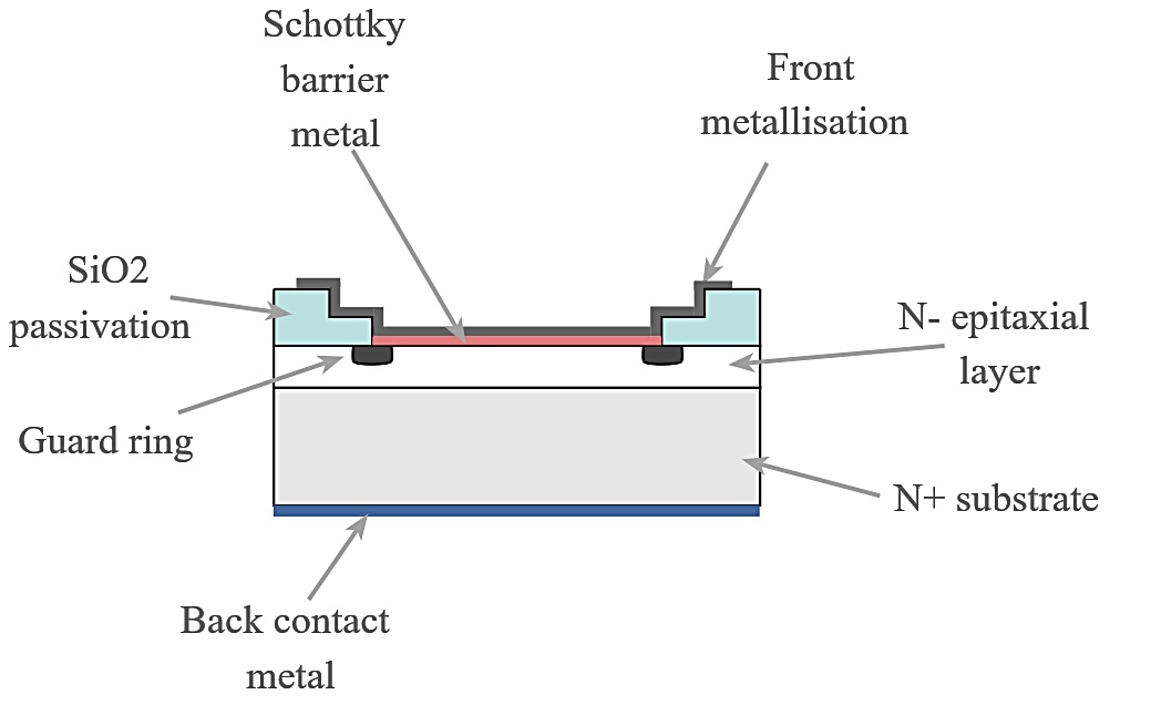
Figure 1
Specifically, when a junction is formed between a metal and a semiconductor it creates a barrier in which an N-type semiconductor acts as a cathode and the metal acts as an anode, effectively forming a diode. This differs from a traditional P-N junction diode in which both surfaces are semiconductors. The behavior of the Schottky barrier changes depending on whether the diode is in an unbiased, forward-bias, or reverse-biased state.
Schottky diodes are fabricated from a semiconductor die to which an epitaxial layer is deposited. While a conventional point-contact diode uses a metal whisker to contact the epitaxial layer forming the rectifying junction, a Schottky diode has an additional oxide layer deposited over the epitaxial layer. An area is etched out through the oxide layer to the epitaxial layer after which a metal contact is deposited.
The benefit to devices using Schottky’s principles is they can be used in a broad array of assemblies such as RF detectors and diode ring mixers at frequencies well into the microwave and millimeter-wave region. Other applications include voltage clamping, prevention of transistor saturation caused by higher current density in the diode, use in photovoltaic systems to prevent batteries from discharging through the solar panels at night, as well as in rectifiers used in switched mode power supplies.
A Schottky diode has much higher current density than a traditional P-N junction, so the forward voltage drop between its terminals when current flows through it is much lower. It typically uses only 300 to 400 mV across its junction, in contrast to a standard silicon diode that has a forward voltage drop of about 600 mV. A Schottky diode also has very fast recovery time between its forward conducting (ON) state and the reverse (OFF) state because it has an infinitesimal amount of stored charge, which in part makes it very well suited for high-speed switching applications as well as RF and microwave applications. In conventional diodes, this time can be several microseconds to less than 100 ns, but as Schottky diodes have no charge carry depletion region at the junction, switching time can be from 100 ps to tens of nanoseconds, that is, almost instantaneous.
Zero-bias Schottky diodes
There are many types of Schottky diodes, one of which is the zero-bias Schottky diode, also known as a Zero-bias Schottky detector diode. This type of Schottky is less susceptible to damage from overdrive, making it more rugged. Whereas a typical Schottky diode has a "knee" on the I/V curve around 300 to 500 mV that limits its low-level signal detection threshold to -20 dBm, a DC-biased, Zero-bias Schottky Diode has a typical knee of 150 mV. This allows them to operate well RF power levels of about 30 dBm.
Zero-bias Schottky diodes are well suited for use as small-signal RF detectors (Figure 2), such as those used in RFID tags and other applications in which no DC power is available in “listen” and other sleep modes.
It is also well-suited for coming generations of IoT devices that operate from coin cell batteries in which conservation of power is critical. Other applications include test equipment, transmitters, signal monitoring, radar, and missile guidance systems. Although they’re not quite as sensitive as, say, a superheterodyne receiver, Zero-bias Schottky Diodes are much less costly and often provide favorable return on investment (ROI). Its only disadvantage is that its performance depends on its saturation current that is directly affected by temperature. But methods have been developed to compensate for this issue.
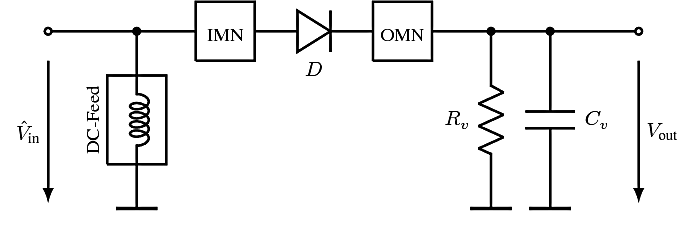
Figure 2
Although the Schottky diode has very few disadvantages, one of them is a higher level of reverse current than a traditional diode. This will lead to more leaked current when connected in reverse. Schottky diodes also have a lower maximum reverse voltage than standard diodes, usually 50 V or less. Once this value is exceeded, the Schottky diode will break down and start to conduct a large amount of current in reverse.
To overcome these problems a guard ring of P+ semiconductor fabricated using a diffusion process is used along with an oxide layer around the edge, which has a positive effect on performance in both forward and reverse directions. Specifically, integrating a guard ring into the device can significantly improve its reverse-breakdown characteristics when compared to the Schottky diode without one.
In short, while Schottky diodes are not a solution for every application, they have distinct advantages that make them the best choice for many, and are likely to be used even more frequently in the future, finding new homes in the tiny devices that will be used in the edge devices in IoT networks. These and the Schottky Diode’s traditional RF and microwave design uses ensure it will have a place in consumer, commercial, and defense systems for years to come.
Check out our other blogs and read "The Ubiquitous Microwave Diode. Chapter 2: PIN Diodes" to learn more about microwave diodes.
Contact our technical support team with any questions.
Captions
1. The Schottky diode, showing its constituent components, in this case including a guard ring. Source: electronics.notes.com
2. A zero-bias Schottky diode RF detector including DC source, input and output networks (IMN and OMN) followed by a low-pass filter. Source: Semantic Scholar.