Metallization
SemiGen offers in house build-to-print services for a wide range of thin film materials and metallization schemes. Our process fab utilizes multiple equipment sets to be able to deploy a wide variety of techniques to meet todays demanding designs. Processes include Filled Vias, Plated Thru Holes, Ion Beam Milling, Sputtering, Photolithography, Electroplating and Dicing. Utilization of our ion beam etch process provides precision line definition and known proven improved performance over high frequency ranges in comparison to traditional chemical etching. SemiGen’s expertise comes from the acquisition of Ion Beam Milling in 2018 and the integration of that technology into our process fab. Services include:
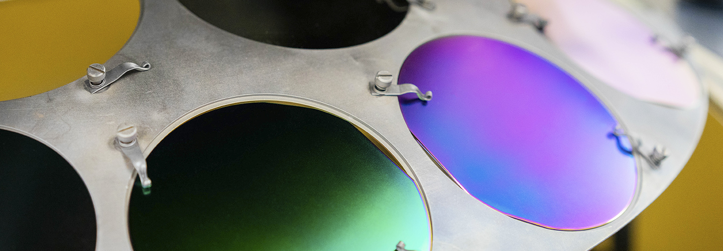
Sputtering
Thin-film manufacturing process for:
- Semiconductor processing
- Precision optics
- Surface finishing
Evaporation
- Filament or e-beam evaporation
Plating
Electro-Plating Finishes Available:
- Soft Gold plating (wire bondable)
- Sulfamate Nickel plating (low stress)
- Copper Sulfate plating for thin film circuits
Metallization Services On:
- Silicon
- GaAs
- Alumina
- Polished Alumina
- Superstrate TPS
- Alumina Nitride
- Beryllium Oxide
- Fused Silica/Quartz
- Saphire
- Hi-K Dielectrics