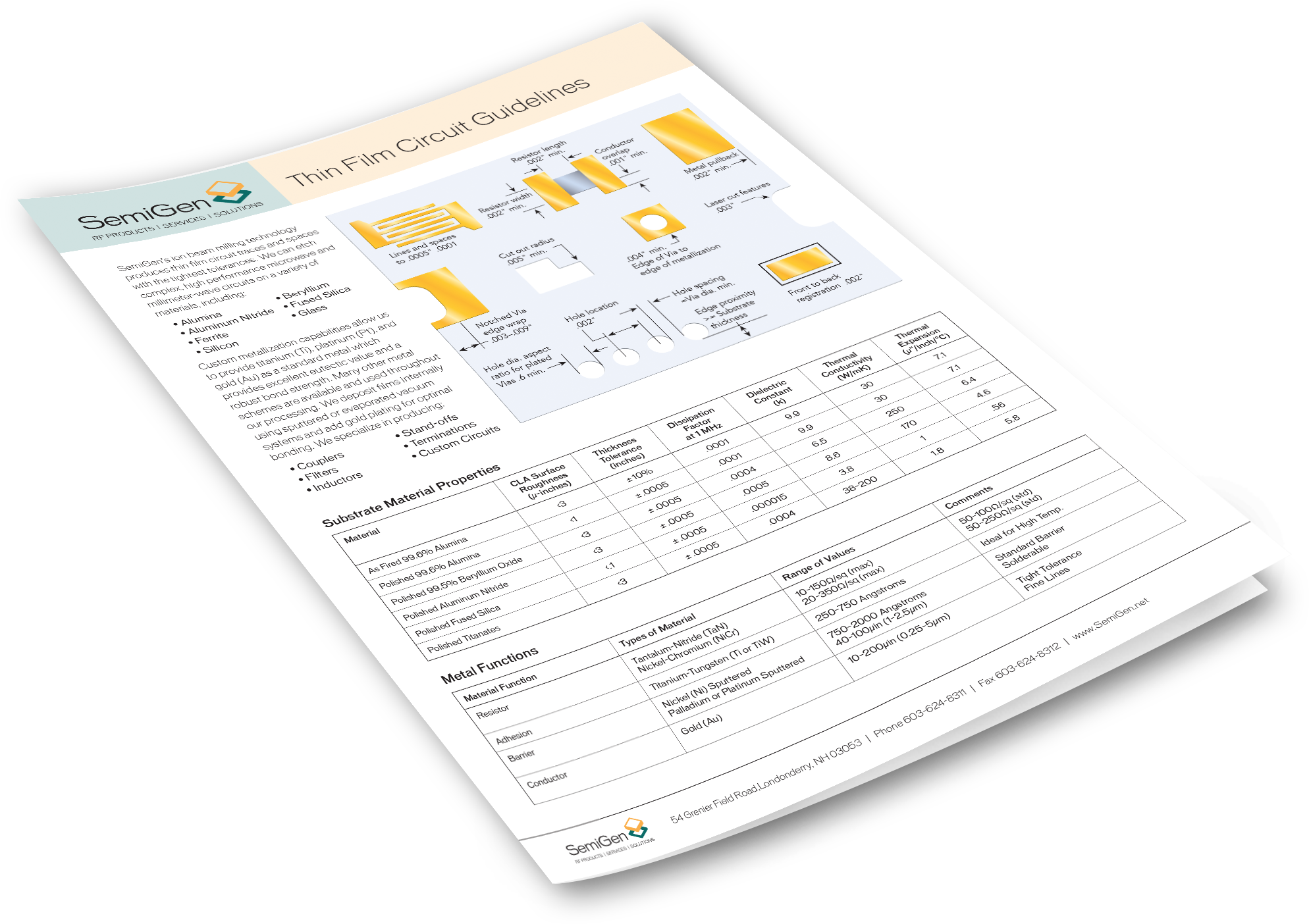
Thin Film Circuits
SemiGen offers build-to-print services for a wide range of materials and metallization schemes. We use our processing technology to fabricate circuits on As-Fired Alumina, Polished Alumina, Superstrate TPS, Aluminum Nitride, Beryllium Oxide, Fused Silica/Quartz, Sapphire, and Hi-K Dielectrics.
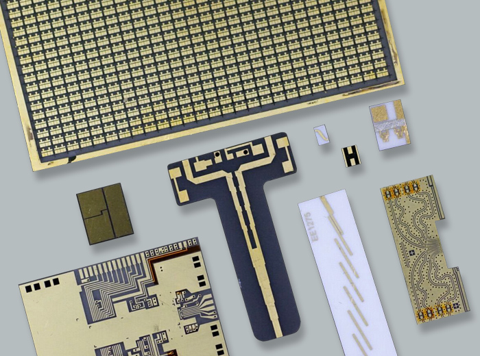
Semigen specializes in the manufacture of Custom Thin Film Circuits and other thin-film products. Circuits can be manufactured to your drawing specifications or we can work with your engineers to design a Thin Film Circuit to meet your requirements.
Our process fab utilizes multiple equipment sets to be able to deploy a wide variety of techniques to meet todays demanding designs. Processes include Filled Vias, Plated Thru Holes, Ion Beam Milling, Sputtering, Photolithography, Electroplating and Dicing. Utilization of our ion beam etch process provides precision line definition and known proven improved performance over high frequency ranges in comparison to traditional checmical etching.
SemiGen’s expertise comes from the acquisition of Ion Beam Milling in 2018 and the integration of that technology into our process fab.
| Substrate Types | Conductor Metallization | ||
| Alumina | >Al2O3 | Resistors-Tantalum Nitride (Ta N) | >20 ö 200 ohms per square |
| Aluminum Nitride | >Al N | Titanium Tungsten Gold | >Ti W Au |
| Fused Silica | >Si O2 | Titanium Tungsten Nickel Gold | >Ti W Ni Au |
| Beryllium Oxide | >Be O | Titanium Platinum Gold | >Ti Pt Au |
| Diamond | >C | Chromium Copper Gold | >Cr Cu Au |
Our metallization capability allows us to deposit:
- Aluminum
- Chrome
- Chromium Copper Gold
- Nickel
- Gold
- Palladium
- Platinum
- Titanium
- Tungsten
- Tantalum Nitride
Whether your requirement is for low volume or production volume, MicroFab is ready to deliver. Our superior Ion Beam Etching process produces accurate and repeatable Thin Film Circuit features, as well as other Thin Film Products that are essential to the high quality our customers expect.
We process with the following substrate materials:
- Alumina- As-Fired and Polished, 99.5% or greater
- Aluminum Nitride
- Quartz/Fuzed Silica
- Sapphire
- Ferrite/Garnet
- Titanates (Hi-K materials)
- Glass
.png)